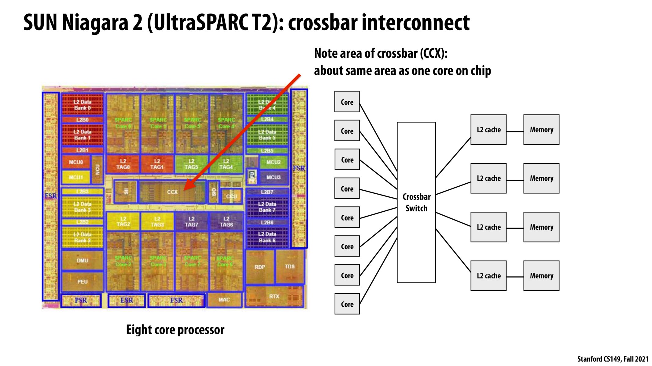


If you want to read more about the processor, you can try this paper: https://www.oracle.com/technetwork/systems/opensparc/02-t2-a-sscc2007-1530395.pdf
Also to answer your first question, I think so... from the paper: "the LSU holds a 4 way set associative level 1 data cache with a 16 byte line size, and a 128 entry data TLB." where the LSU (load/store unit) is part of a single core.
To answer your second question: here's another excerpt from the paper: "The eight SPARC processor cores share an 8- banked, 4MB Level 2 cache (L2). Each bank of the L2 cache is 16-way set associative with a line size of 64 bytes. The eight banks of L2 allow eight simultaneous accesses to support the high bandwidth requirements of UltraSPARC T2." There's more to it than this, so if you're interested would definitely recommend the paper.
To answer the last question about the L3 cache, I don't think it actually has a L3 cache... There's no hard requirement on how many levels of cache you need, in fact I think the first CPU to use a cache only had 1 level of cache. I think it's also pretty common in GPU architecture to not have a L3 cache, just L1/L2 (https://developer.nvidia.com/blog/cuda-refresher-cuda-programming-model/).

Honestly tho, why are microprocessor images always blurred? Is it because of proprietary reasons?

Microprocessors are made with multiple layers of silicon, and I would assume that the images are blurred because X-rays are used to image the chip, and the upper layers are somehow interfering.
What interests me about this processor is why is there a separate L2 cache for each memory controller instead of one large L2 cache with higher set associativity. I suppose it is faster to search 4 smaller caches than one larger cache, but highly threaded applications which use an address space which maps to only memory controller will fill up the L2 for that memory controller and incur many more cache misses.
Please log in to leave a comment.
Looking on the diagram on the right, each core has its own L1 cache, that is why it is not displayed, right?
Moreover, from the diagram we see that 8 cores share 4 L2 caches. I was wondering what is the eviction policy for these L2 caches. Also, are the L2 caches specifically assigned to a batch of cores (like 1 L2 cache per 2 cores), or all cores can read and write to all L2 caches.
Finally, for this processor, where would the L3 cache be?